


JAN / JANTX/ JANTXV / JANS / JANSR
1N / 2N / DG Part Types
Small Signal and Power Diodes
Transistors / MOSFETs / JFETs
Silicon Controlled Rectifiers
Analog Switches
Leadtimes 6 to 26 Weeks!
Also Available:
✓ Custom Configurations
✓ Lower Cost Non-JAN
✓ DIE Form (With Free Element Evaluation)
💥Many Items In Stock Today!💥
Diodes
VPT Components
JFETs
VPT Components / Siliconix Inside
MOSFETs
VPT Components / Siliconix Inside
Transistors
VPT Components
For detailed PRODUCT INFORMATION about BARE DIE COMPONENTS
and the world class manufactures who make them, CLICK HERE.
What Is Bare Die?
What is Bare Die? Where is it used? What are the benefits of using Bare Die? These are questions that many design engineers and buyers ask. Unless you have been doing this for a good number of years you will quickly find out that there is a lot more involved than just searching for a Part# on the Internet. The trick is understanding the differences between packaged parts and bare die. Bare Die is used in a broad array of industries, and markets, including Aerospace, Military, Avionics, Medical Implant, Automotive, and high-end Industrial where bare die is the optimum choice for a given design.
Section 1:
Reasons To Use Bare Die
Smaller Size and Weight - Using bare die can allow for reduced board space.
Operating Temperature Size - Package thermal characteristics no longer inhibit the performance of the die or the environments where they can operate.
Ruggedness - Direct die attach and wirebond provides protections against high levels of shock and vibration.
Lighter Weight - Smaller designs and higher densities reduce weight and size of your application.
More Efficient Performance - Removing extra package interconnect can reduce capacitance and inductance.
Reliability - The reduced number of interconnects with die use leads to improved reliability. The typical packaged part has three connection points per I/O. Compare this with only two for wire bonds.
Electrical Performance - The lower inductance and capacitance of bare die is important in analog, RF, and power applications. Faster signal flight time (lower propagation delay) and improved power/ground distributions.
Hermetically Sealing - Air tight sealed packages can be selected that can be injected with inert gasses.
These die advantages promote higher levels of integration, improved electrical and reliability performance, and increased functionality per square area. The benefits of using unpackaged die in embedded designs can be substantial. The availability of IC products in die form gives customers a convenient option for small-footprint designs, enabling them to optimize their product designs for limited space and to implement innovative, proprietary packaging solutions.
Section 2:
----------OUR TOP 10 BLOGS----------
The Secret of Specifying and Obtaining the Correct Bare Die to Build Hybrid Microcircuits
What is Bare Die? How do I buy Bare Die?
Unless you have been doing this for a good number of years you will quickly find out that there is a lot more involved than just searching for a Part# on the Internet. It’s especially frustrating to find out that in a world of “packaged” semiconductors that Bare Die commerce is perceived as a bother. The trick is understanding the differences between packaged parts and bare die.
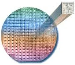
SILICON Wafer
Manufacturers produce a wafer that yields the die. After testing the wafer, individual die are separated from the wafer and assigned a part number and then shipped to a bare die distributor. Here, samples from a die lot are packaged to expedite Lot Acceptance Testing (LAT). Additional testing is usually done through a method of Known Good Die (KGD).
First, find a trusted Bare Die supplier that can provide you with the components in die form. Their expertise and advice will help you in the buying process. You may need Certificates of Conformance, Lot Traceability, Source Control Drawings, Geometries, Specific Testing performed. It can be very confusing.
Manufacturers produce a wafer that yields the die. After testing the wafer, individual die are separated from the wafer and assigned a part number and then shipped to a bare die distributor. Here, samples from a die lot are packaged to expedite Lot Acceptance Testing (LAT). Additional testing is usually done through a method of Known Good Die (KGD).
At the distributors facility, the die is visually reinspected to make sure that the die that you purchase looks flawless and will function well. In some instances, additional electrical testing is also performed for screening of specific electrical parameters. Current die geometries must be obtained and any changes that have occurred must be forwarded to the end customer for review and approval. Often times samples are required by the end customer. Depending on the device, the distributors can usually provide the required sample. Sometimes though, the part is not available from the manufacturer in die form, or if the manufacturer agrees to provide the part, the minimum purchase quantity may be much, much higher than the end customer requires. Always keep in mind that everything is NOT available in die form.
Specifying and obtaining the correct bare die to build hybrid microcircuits and multi-chip modules presents some specific problems. Dominant design factors here are hermetic sealing requirements, size, and weight. However, the special needs related to the supply of bare die continues to mystify much of the electronics community beyond the handful of hybrid manufacturers specifically focused on this market.
Most hybrids are designed around the characterization of packaged parts. Once samples are received, the function designer builds the breadboard, runs characterization data, and then asks the hybrid designers to create a hybrid or multi-chip module to simulate the function. Here is where the die distributor immediately begins to add value.
Taking the Bill Of Materials (BOM) from the customer, we immediately determine which of the requested parts are not readily available in die form or require added value processing. First, some semiconductor devices are not available as bare die because the manufacturer simply elects not to offer the device in die form. Many newer power discrete devices are assembled in packages that use a braised clip for the top contact attachment point. The top metal used to facilitate these packages is not suitable for wire bonding or soldering, so the manufacturer will not offer this die to the market.
In this era of large wafer diameters of 6-in. or 8-in. and larger, the manufacturer may elect not to 100 percent-probe smaller die at the wafer level. The manufacturer does sample probes only, and accepts the predicted yield loss during 100 percent test of the packaged part.
In some cases, parts that have no prior history in the die market may have prohibitively high minimum order requirements in die or wafer form from the manufacturer, making it impossible to sample or support prototype builds.
The die distributor can address each of these problems and either perform the required added value or recommend a list of alternatives that are more readily available. In the case where a manufacturer will simply not quote a bare die, the die distributor often has access to alternative sources that can offer die with similar functions.
Suitability for Wire Bonding
Where the top metal is not suitable for wire bonding, it is usually not difficult to find a similar device within the vendor portfolio that is offered in die form with the preferred metallization. In the case where 100 percent probe is not performed by the manufacturer, the die distributor can offer this service using in-house capabilities or outsourcing to an approved test lab. This also involves the distributor performing a Lot Acceptance Test (LAT) after probe, to provide objective evidence that the probe successfully met the specified requirements.
Stocking and Inventory Control
At ES Components, we have proactively identified a long list of popular devices throughout our line card and established an “off-the-shelf” inventory. This inventory is automatically replenished based on a predetermined min/max rather than market demand. An off-the-shelf part is immediately available for sampling and has virtually no Minimum Order Quantity (MOQ) when supporting prototype procurements. The products offered include a variety of analog microcircuits and a compete portfolio of popular discrete die and thin film resistor chips. We use this preferred inventory to quickly offer the hybrid designer alternatives that are readily available and provide a cost-effective solution. If the customer is unable to use one of these devices, we then support the procurement of a different required device.
Are you soldering to the top contact or wire bonding?
This is a must if there are any power discrete devices on the BOM. Many discrete die are available with either option. The rest are only offered with one or the other of these two options. If only solderable top metal is available, and there are no alternative devices, the die distributor can possibly offer a sub-assembly using a Copper or Molybdenum disk with suitable top plating to meet wire bond requirements.
How are you planning to attach the die?
The vast majority of power discretes are available from the manufacturer with solderable back metal only, some with either solderable or gold back metal. If the user is planning to use epoxy attach, it is highly recommended that they not use die with solderable metals. Gold back metal is recommended for either eutectic or epoxy attach. At ES Components we have developed and qualified the ability to remove solderable back metal from wafers and deposit gold for devices where this option is not available from the vendor. Silicon back die are generally epoxy-attached and if a eutectic attach is required, a gold alloy preform is needed.
How will you want this bare die packaged for delivery in full production?
Packaged parts are typically supplied in production quantities on tape-and-reel with nearly infinite shelf life. Waffle packs are the most common medium for shipping bare die, but high volume automatic assemblies are moving towards sawn wafer on film to reduce cost and enhance manufacturing throughput. However, sawn wafer on film has shelf life limitations which demand special management of the supply pipeline. A die distributor can manage the pipeline so that probed unsawn wafers are kept in stock in the appropriate environment and sawn wafers on film are limited to only those wafers needed for short-term production. If there is a delay in manufacturing, the unsawn wafer inventory remains pristine and the shelf life issue is confined to a small subset of the inventory.
Summary
By answering these questions at the time of initial contact and early in the design process, it’s possible to save the user time and money by avoiding the need to modify or redesign the function based on sample evaluation possibly weeks or even months later. We can also properly code the die part number to capture all the pertinent information for future reference.
ES Components is a trusted Bare Die supplier that will help you obtain the expertise and advice you need to buy bare die.
Section 3:
Assembly Options for Hybrid Packaging
What Is Bare Die Bonding?

Diagram of how DIE is attached and Bonded
Definition
Die bonding (often referred to as die attach) is the process of attaching a die/chip to a substrate or package. Die attach is accomplished by using one of the following processes:
Eutectic
Solder
Adhesive
Glass or Silver-Glass
For our purposes here we will focus on Eutectic, Adhesive and Silver-Glass.
Eutectic Bonding


Eutectic DIE Attach
A eutectic bond is formed by melting a preform consisting of a mixture or alloy of two or more dissimilar metals in the joint between the die and substrate. In some cases the die may have a eutectic alloy pre-plated on its back omitting the need for a preform. The preform has a melting point which is lower than the melting point of its base materials. Consider a typical preform composed of gold and silicon. The melting point of gold is 1640° C, and the melting point of silicon is 1414°C. However, when the materials are combined into a preform, the melting point becomes 363° C.

PROS and CONS
In the eutectic process, the substrate is secured on a heated workstage which operates at a temperature just below the eutectic melting point. When the die and preform are placed on the substrate, the bonder initiates a light scrubbing action with the bond head. This scrubbing generates just enough energy to raise the temperature at the bond site above the eutectic melting point. When scrubbing ceases, the melted material solidifies, thereby creating the bond. Nitrogen is used as a cover gas in order to prevent oxidation due to the high heat.
Adhesive Bonding

Adhesive Die Attached
An adhesive bond is formed by adhering the die to the substrate using some type of adhesive material. It can be electrically insulating or conductive depending on the adhesive material used. Adhesive bonds are conducted at room temperature.

PROs and Cons of Adhesive DIE Bonding

In the adhesive bonding process, the substrate or package is secured to an unheated workstage. The adhesive material is contained in a reservoir and a small amount is metered out onto the substrate, usually in a pattern conforming to the shape and size of the die. The bonder then picks up the die and places it on the adhesive, making the bond. The bond process is complete once the adhesive dries.

PROS and CONS of Silver Glass Bonding

In the adhesive bonding process, the substrate or package is secured to an unheated workstage. The adhesive material is contained in a reservoir and a small amount is metered out onto the substrate, usually in a pattern conforming to the shape and size of the die. The bonder then picks up the die and places it on the adhesive, making the bond. The bond process is complete once the adhesive dries.
Glass /Silver-Glass Bonding
A glass bond is formed by adhering the die to the substrate using glass in the form of a paste. The glass paste may also contain silver particles which enhance thermal and electrical conductivity (this is what is called Silver-Glass die bonding).
The Glass bonding process is similar to Adhesive bonding. The differences are the material used and the need for heat. Glass bonds are heated to 350-450°C which melts the glass into a low viscosity liquid. The glass hardens as it cools thereby making the bond.
Section 4
How Bare Die is Handled to Ensure Long-term Reliability and How it is Delivered
Handling Bare Die can be tricky. The following should help raise the sensitivity and awareness of special physical effects which could harm the quality and yield of the production of bare die.
Bare Die Is Delivered In Different Forms

Unsawn Wafer

Sawn Wafer

How Die is marked after Testing, Partially Picked Frame Carrier (PFC). Chips Not In Spec Are Marked With An Ink Dot

Die on Tape and Reel

BAre DIE in a TRAY
Handling Consideration to Ensure Long-Term Reliability
Electric Fields & Overvoltages
Mechanical Damage
Surface Contamination
Electrical Fields
Chips are protected against ElectroStatic Discharge (ESD) up to a certain level defined in the Quality and Reliability Specification (QRS) and circuit specification. Depending on the design of the device protection, the ESD protection can reach values up to some kV limit.
Electric fields are mostly generated by moving objects or persons. A person, for example walking on a carpet, can easily be charged up to 35 kV (see Table 1). Not only high voltages, but even small electric charges can be sufficient to damage sensitive electronic components. Devices which have been exposed to a certain electrical field may not be destroyed but the reliability of the IC may be affected. Therefore it is necessary to handle bare die in a electrostatic protected environment.

Sources of Static Electricity that can Damage DIE
Damage To Sensitive Electronic Components

AN Example of a DIE that has been damaged by static electriciity
Surface Contamination
Interconnection and molding steps are very sensitive to microscopic and macroscopic surface contamination. Contaminated surfaces can be the reason for issues during assembly and can also lead to long-term reliability problems.
Work Place Requirements
Clean room
Bare die must always be handled in a clean room environment of at least class 1000 (ISO 6) or better. A clean room is an environment that has a controlled level of contaminates, such as dust, aerosol particles or microbes. They are used in laboratory work and in the production of precision parts for electronic or aerospace equipment. The level of contamination is classified by the number of particles at a certain size per cubic feet or cubic meter.

Clean Room Classes for DIE Handling

Clean Room Classes for DIE Handling
The external and internal air for the clean room is filtered through high efficient filter systems to exclude particles and remove internally produced contaminates. Entering the clean room has to be done by passing an air or vacuum shower to remove adherent particles.

Entering A Clean Room Through A Vacuum Shower

Staff, working in the clean room has to wear special protective cloths: heads, face masks, gloves, boots and cover-alls
All equipment used in a clean room has to be designed to avoid emissions.
Special supplies are available for example:
Clean room ball point pen, which have low-sodium ink to provide protection from ionic contamination (pencils and erasers are not allowed in clean rooms)
Clean room paper which is designed not to emit particles
Clean room binders, which are solvent resistant
Electrical grounding
Every possible device which could be in contact with the die must be on the same electrical potential, this is also true for the operators dealing with the equipment. To achieve this, everybody and everything must be grounded to the same electrical potential.
Dedicated equipment is readily available:
Grounded workbench surface
Conductive carpets
Grounded chairs
Low impedance place mats
Grounding wrist straps
ESD safe shoes, coats, gloves and finger cots
The goal is to avoid the development of an electrical charge that could cause a potential damaging electrostatic discharge.
Special working behavior
Access to clean room areas should be limited to persons necessary for the area operation.
Eating, drinking, chewing gum and smoking is not allowed in clean rooms.
Nervous relief type mannerisms such as scratching the head, rubbing hands or parts of the body, or similar type action are to be avoided.
All material can only be moved from one clean room to another in the same or lower clean room class, but never in the other direction.
Die Handling
Bare die must be handled always in a class 1000 (ISO 6) clean room environment: unpacking and inspection, die bonding, wire bonding, molding, sealing. Handling must be reduced to the absolute minimum, unnecessary inspections or repacking tasks have to be avoided. Use of complete packing units (tray, FFC, tape and reel) is recommended and remaining quantities have to be repacked immediately after any process (e.g. picking) step. To avoid contamination and damages (scratches, cracks)
Bare Die or wafers must never be handled by bare fingers
The active side of a Bare Die should never be touched
The mechanical pressure has to be limited
Do not store and transport Bare Die outside protective bags, tubes or boxes
Work only in ESD safe clean room environments
Tools used to safely move DIE without damage
Special tweezers are suitable for grabbing die and wafers on its edge. Vacuum tweezers are used to move die from the packing to the target.

Vacuum Pick Tool

The Vacuum pick up tool

Special Tweezers For Grabbing A Wafer
Packaging

DIE Stored in an Aluminum (Anti-Static) Vacuum bag injected with Nitrogen (Inert Gas)
Transport Conditions
General transport conditions
During transport, the packing and the products have to be protected against extreme temperatures, humidity, direct sunlight, and mechanical forces. The temperature has to be between 8 °C to 60 °C. The total transport time should be as short as possible. When the transport time exceeds five days, the transport conditions must be the same as the store conditions.
Conditioned air transport
For dry pack, conditioned cargo rooms are mandatory for air transport. The temperature has to be between 8 °C to 45 °C with an average humidity of 16 %. The air pressure has to be between 700 hPa to 1060 hPa.
General store conditions
Secure and clean store areas shall be provided to isolate and protect the products. Conditions in the store areas shall be such that the quality of the products do not deteriorate due to harmful gasses or electrical fields.
The following conditions have to be maintained:
Temperature between 8-45 degrees centigrade
Humidity between 25% - 75%, no condensation under any condition allowed
No exposure to direct sunlight
Die are best stored in the package as delivered. Chips on film frame carrier (FFC) will stick stronger on the foil with time and will require more effort to pick them off the foil. In the worst case, some residual foil (glue) might stick on the rear side of the die.
Storage conditions if not packed in dry pack
If wafers and bare die are not packed in dry pack, they have to be stored under the following types of conditions: inert gas (nitrogen), nitrogen flow boxes, and with a relative humidity below 30% and temperature between 18 °C to 24 °C.
Shelf life
The shelf life is the possible storage life before the product is used.
Typically shelf lives are:
Bare Die in tray - 3 years
Wafer on FFC - 0.5 years
Unsawn Wafer - 3 years